Target Processor CPU Usage Models
This chapter consists of the following sections:
- PowerPC CPU Usage Model
- MIPS I CPU Usage Model
- MIPS II/III/IV/64 CPU Usage Model
- Honeywell RH32 CPU Usage Model
- M68000 CPU Usage Model
- i386 Family CPU Usage Model
PowerPC CPU Usage ModelThe following sections describe how TDM and the Apex Embedded kernel use the PowerPC and its FPU. It also lists some precautions to take when writing machine code for the PowerPC.
- Register Conventions
- Machine State Register (MSR) Usage
- Software Floating Point
- Software Floating Point Parameter Passing Conventions
- AltiVec Usage
Much of the design described in this section is embodied in the code in the kernel configuration area. In particular, the file v_krn_conf.2.ada contains all of the source code for the trap handlers. The constant and type definitions describing the registers and other processor data structures are in the file v_cpu_conf.1.ada, in the rational.ss subsystem.
Register Conventions
Apex Embedded for the PowerPC uses the register conventions defined in the Motorola Embedded Applications Binary Interface (EABI).
Machine State Register (MSR) Usage
Apex for Rational Exec requires the MSR to use big-endian byte ordering, so LEV (bit 31) must be set to 0. Also, all application tasks must execute in supervisot state, so PR (bit 17) must be set to 0.
Otherwise the rest of the bits in the MSR can be customized to your application. The default settings while user code is executing is:
Software Floating Point
Rational supports the MPC860 variant of the PowerPC. The MPC860 is similar to other implementations of the PowerPC but does not have hardware support for floating-point operations. Floating point operations are done with software.
There must be a separate instance of all the standard views (lrm, predefined, etc.) so that any compiled code which uses floating point operations does not attempt to use floating point hardware.
Views that work with PowerPC chips with hardware floating point have the compiler_variant identifier rx_ppc and views for chips like the MPC860 which do not have hardware floating point are identified with compiler_variant rx_ppcsfp (RationalExec_PowerPCSoftwareFloatingPoint).
Note: If your system requires floating point math, a separate archive of code and a license must be obtained from U.S. Software that implements the floating point functions (add, subtract, multiply, divide, conversions from int to float, and from float to int, etc.) The archive is called gofast.var and is sold independently of Rational Software.
Contact your Rational sales representative for assistance or Call U.S. Software at (800) 356-7097.
After obtaining the gofast.var archive it must be copied into the location in the Apex installation with the other runtime archives:
Apex ships with a "dummy" version of gofast.var in the archive directories described above. The dummy gofast.var prevents the linker from complaining that it cannot find gofast.var. Safely replace the dummy with the real gofast.var once you obtain it from U.S. Software. (Note that the dummy archive is much smaller than the real one.)
It is not necessary to have the real gofast.var to link the kernels and TDMs shipped with Apex. However, if the kernel or TDM is changed to use floating point operations then the real gofast.var is needed to link them.
The real gofast.var is not needed to link user applications that do not use floating point. However, beware that ada.text_io as shipped in Apex Substitute version number here requires floating point. If simple I/O routines are needed for debugging and do not have the real gofast.var try the package simple_io.
Rational provides the BSP mpc680ads for the Motorola mpc860ads board which uses the MPC860 chip. This BSP supports serial TDM and the Agilent software probe.
Software Floating Point Parameter Passing Conventions
Using the GNU C compiler for the mpc860 target with software floating point:
- 1 . Registers r3-r10 are the int/float parameter registers.
- 2 . For 32-bit ints, registers r3-r10 are used consecutively. When exhausted, we use increasing mod 4 locations beginning with 8(sp).
- 3 . For 64-bit ints, registers r3-r10 are used pairwise (r3/r4, r5/r6,...). The first register can be odd or even numbered (so r4/r5 is a legal pair). If only register r10 is available, we skip it and store the long pair on the stack. Stack locations are mod 8 beginning with 8(sp).
- 4 . For 32-bit floats, registers r3-10 are used in the same manner as for passing 32-bit int arguments. Stack locations are mod 4.
- 5 . For 64-bit floats, registers r3-10 are used pairwise identically in the manner employed for 64-bit ints. Stack usage differs slightly. Stack locations for 64-bit floats are mod 4, not mod 8.
- 6 . 32-bit values are returned in register r3. 64-bit values are returned in register pair r3/r4.
AltiVec Usage
Overview
Note: AltiVec is a trademark of Motorola Corp.
Some variants of the PowerPC chip (currently the MPC7400) contain an SIMD unit which follows the Motorola AltiVec standard.
Rational Apex Embedded for the PowerPC supports AltiVec in several ways:
- 1 . The package System.Machine_Code contains all of the AltiVec-specific opcodes and registers.
- 2 . The Apex debugger and disassembler disassemble AltiVec instructions.
- 3 . The target debug monitor (TDM) has some added "pass-through" command capability to allow you to examine the contents of the AltiVec vector registers during debug.
From a programming perspective, access to the AltiVec is provided through Ada machine code insertions, which is similar to assembly-level programming. The Motorola manual "AltiVec Technology Programming Environments Manual (doc # ALTIVECPEM/D)" which can be found on Motorola's literature web site in PDF format is a valuable resource for programming in AltiVec assembler.
Initialization
To initialize the AltiVec, you:
- 1 . Set the VEC bit in the Machine State Register (MSR, bit 6) to 1.
- 2 . Set the AltiVec's NJ bit in the Vector Status and Control Register (VSCR, bit 111) to 1. See the section labeled "The Non-Java Bit" as to why you should set NJ.
This initialization can be done either in the kernel's start up code, V_Krn_Conf.V_Start_Program, or in the user's application. The only requirement is that the initialization must occur before the AltiVec is used.
Programming the AltiVec
Programming Example
For reference, an AltiVec programming example is provided in the release as test_3d.2.ada and three_d_coordinates.[12].ada in the ada_examples.ss view of the MVME5100 BSP.
The package three_d_coordinates.2.ada, contains an example of the required initialization code mentioned in the previous section. The routine's name is Enable_Altivec_Support. It also contains a non-trivial example of using the AltiVec instruction set via Ada machine code insertions.
The Non-Java Bit
The Non-Java (NJ) bit in the VSCR needs to be set to 1 so that denormalized results will not cause the AltiVec to issue a trap. Denormalized results are not handled by the AltiVec hardware, so it generates a trap that could be handled by system software that would emulate the operation, producing the correct denormalized result. This, unfortunately, would cause a large performance hit. Because of this, in Apex we've chosen not to implement the denormalized number emulation in the system software. In order to disable the denormalized number trap and set the result to 0, the NJ bit must be set. If you do not set the NJ bit, you may encounter an unhandled trap panic at runtime.
There is an example of code that sets the NJ bit in the programming example mentioned in the previous section. The routine is Three_D_Coordinates.Set_Nj_Bit_In_Vscr.
Alignment of Vector Objects in Memory
In order load and store vectors from memory, there are essentially two choices:
- 1 . Always load and store vector objects to memory aligned on 16-byte boundaries using a single-instruction load or store (Lvx, and Stvx).
Note: Using these same instructions on addresses which are not 16-byte aligned will cause the AltiVec to load the data starting at the address specified, but adjusted down to the nearest 16-byte boundary. This will cause the wrong data to be loaded, and data to be stored at the wrong location possibly overwriting other variables. What's worse is that if you do not align the data, you may get lucky and have it correctly aligned, but small changes to your program will disturb the alignment resulting in erroneous program behavior for what appears to be an innocuous change.
- 2 . Load and store vector objects which lay on arbitrary boundaries using a longer instruction sequence.
Because option 2 is much slower and not described well in the Motorola documentation, particularly for an unaligned store, Rational recommends that you use 1 instead.
Given that you want to align vector objects on 16-byte boundary, you have three alternatives:
- 1 . Apply an alignment clause to an object declared in a static scope (a.k.a. library-level object): "for <object>'Alignment use 16;"
An object declared in a static scope would be in a package that is declared at the library level and the object is not inside any dynamic scope enclosure (such as a subprogram).
The downside of this alternative is that since the object must be in a static scope, it can make the code harder to write because now, in essence, you are programming with global variables.
- 2 . Declare a buffer in a dynamic scope that's large enough to align the vector within it. For example:
A disadvantage of this method is that the code is a bit more complex looking.
- 3 . Create your own storage pool for Vector objects, and this pool would always return 16-byte aligned vector objects. To get a new vector, you just use an Ada "new" operator. A disadvantage is that storage pools require more runtime overhead than 2).
Context Switching the AltiVec Register Set
The AltiVec contains 32 vector registers. These vector registers are not saved and restored neither in interrupt handlers nor across task context switches. Therefore, several usage models are possible (in order of increasing complexity):
- 1 . Designate a single task responsible for using the entire AltiVec.
- 2 . Designate multiple tasks to each use their own subset of the registers. For example, two tasks, A and B, could share the register set by allocating registers 0..15 to task A and 16..31 to task B.
- 3 . A mutex or an Ada protected object could be used to provide mutual exclusion to the AltiVec so that it could be used from any number of tasks. This has the disadvantage of strictly serializing access to the AltiVec.
- 4 . Some combination of 2) and 3). For example, tasks A and B could serialize access to registers 0..9, while task C has exclusive access to registers 10..31.
Install a Task_Switch_Event callout via V_Xtasking.Install_Callout (contained in the rts_vads_exec.ss view) to save and restore AltiVec context for every task.
Debugging AltiVec
Debugging using serial TDM
If you use the version of Serial TDM that comes with the MVME5100 BSP, that TDM supports several "pass-through" commands which aid in debugging of the AltiVec's register set.
The syntax for displaying the AltiVec Vector Registers in TDM is similar to that of the conventional Apex debugger commands, but you need to add the word "pass" in front of it. The syntax is
where NN is in the range 0..31
For example, to display vector register 15, you use this command:
The format in which the pass-through command will print out the register is dependent upon the current setting of vector format, and obase, which also must be set with a pass-through command.
For vector_format, the syntax is:
For obase, the syntax supported is:
In the mode set above, the output for "pass p $vr15" might look something like:
As shipped, TDM allows only reading AltiVec registers, not writing them. However, if you want, you could add the writing functionality to v_tdm_conf.altivec_and_spr_passthru.2.ada in the tdm_conf.serial view of the MVME5100 BSP; all of the parsing of pass-through commands and the accessing of the AltiVec register set is done from there.
This version of TDM also allows reading of arbitrary Special Purpose Registers (SPRs) on the processor. This is particularly useful for SPR registers which are not currently visible without using a "pass" command. The syntax is:
where NNNN is in the range of 0..1023, e.g.:
Debugging using the Agilent E5900B Probe
The E5900B Agilent probe also allows you to examine the AltiVec register set during debug, but the commands are different from the ones supported in TDM. To display a vector register, use this syntax:
where NN is in the range of 0..31, e.g.:
The register will print out in hex (always) and look something like the following:
As you can see, that is a bit harder to read. Currently, it is the only option, however, when using the probe.
The probe does allow you to write AltiVec registers using the syntax:
pass reg vrNN=################################, e.g.:
MIPS I CPU Usage ModelThe following sections describe how the MIPS R3xxx and its FPC are set up and used by TDM and the kernel. It also describes interrupt and exception handling.
- Overview
- Initialization
- Floating Point Coprocessor (FPC) Support
- CP0 Status Register Usage
- CP0 Status Register Usage
- Memory Management Support
Note: The user manual for the MIPS chip you are using is a good reference.
Overview
The R3xxx series chips are an implementation of the MIPS I RISC architecture.
The MIPS I architecture supports two modes of execution, user and kernel. Programs running in user mode are restricted as to what memory and coprocessors can be accessed.
Many of the MIPS I chip implementations allow the processor byte order to be either little endian or big endian. On the most chips, this is specified at power-up by hardware. Also, most chips allow the endian-ness to be reversed by the kernel for code that runs in user mode. Apex Embedded supports execution in either endian mode with separate predefined views. However runtime endian-ness switching is not supported by Apex Embedded, since it requires that programs run in user mode.
Initialization
When the R3xxx chip is reset, it immediately jumps to the reset exception vector at address 16#BFC0_0000#. This fixed address is near the end of kseg1 and is defined by the chip architecture. When the kernel or TDM is placed in ROM, a branch instruction is placed at this address to cause the processor to jump to the beginning of the program.
Because the R3xxx architecture is fixed in many ways, and since Apex Embedded does not use virtual memory, very little initialization needs to be performed to get the processor going. Initialization consists mainly of initializing the CP0 status register and initializing the caches.
Floating Point Coprocessor (FPC) Support
The R3xxx's FPC, has limited floating point capability. It supports only the basic arithmetic operations on floats: +, -, *, /, abs, unary - and some format conversions.
The FPC is capable of handling operations on numbers in a restricted size range, that is, a smaller range than the IEEE specification. Also, it does not handle denormalized numbers or the IEEE exception cases (infinity, NaN, etc.). In these cases, the FPC causes a trap to the kernel. The kernel has routines, supplied by MIPS Computer Systems, Inc., for the software emulation of FPC operations to the full IEEE specification. If there is no FPC on the board, this emulation software is used to emulate all floating point operations.
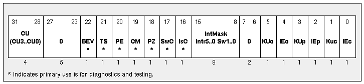
CP0 Status Register Usage
The layout of the CP0 status register is shown in Figure 11. This figure is taken from the 1988 edition of Gary Kane's MIPS RISC Architecture. It includes a breakdown of the diagnostic field. It is included for your reference.
- The processor interrupt mask is changed via the following instruction sequence:
Since the above sequence is executed with interrupts enabled, it can be interrupted. As a consequence, interrupt handlers must restore c0_status to its original state before returning.
- The IEc (Interrupt Enable current) bit should not be used for disabling/enabling interrupts. Use the Intr5 .. 0 and Sw1 .. 0 bits instead.
- The IEo (Interrupt Enable old) bit is lost when an interrupt occurs, so it cannot be relied upon to stay the same between any two instructions unless all interrupts are disabled.
- The Cu1 bit is used by the floating point support code, so it should not be changed.
Figure 11 The MIPS I Status Register
Memory Management Support
The memory map of most R3xxx chips is shown in Figure 12 This figure is taken from the 1988 edition of Gary Kane's MIPS RISC Architecture Manual. We include it for your reference. The map may vary somewhat on some variations of the MIPS R3xxx chips, because some do not have a TLB.
Figure 12 MIPS I Virtual Memory Map
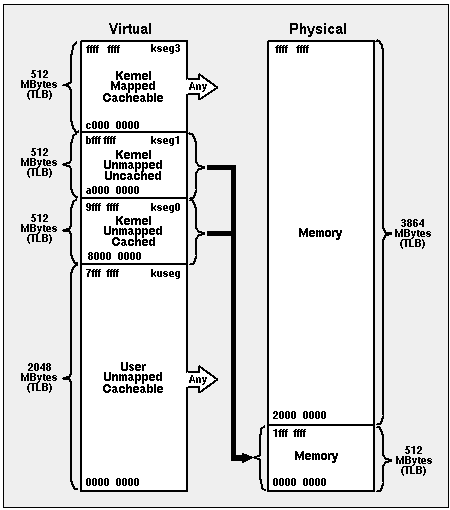
Apex Embedded currently does not support virtual (paged) memory. All code written for Apex Embedded runs in kernel mode in kseg0 (addresses 16#8000_0000#. 16#9FFF_FFFF#) which is cached and directly mapped to physical memory locations 0 .. 16#1FFF_FFFF#. We do not support programs executing in user mode since they cannot access kseg0.
For additional information about memory management in Apex, see "Memory Management" in the Ada Runtime Guide.
MIPS II/III/IV/64 CPU Usage ModelThe following sections describe how the MIPS II/III/IV/64 is set up by TDM and the kernel.
- Overview
- Initialization
- Floating Point Coprocessor (FPC) Support
- CP0 Status Register Usage
- Memory Management Support
- Accessing the Translation Lookaside Buffer (TLB)
Note: The user manual for the MIPS chip you are using is a good reference.
Overview
Most of the MIPS II/III/IV/64 chip implementations support three modes of execution: user, supervisor and kernel. Programs running in user or supervisor mode are restricted as to what memory and coprocessors can be accessed.
Many of the MIPS II/III/IV/64 chip implementations allow the processor byte order to be either little endian or big endian. On the most chips, this is specified at power-up by hardware. Also, most chips allow the endian-ness to be reversed by the kernel for code that runs in user mode. Apex Embedded supports execution in either endian mode with separate predefined views. However, runtime endian-ness switching is not supported by Apex Embedded, since it requires that programs can in run user mode. See "Getting Started" in the User's Guide for more information on choosing the right target library.
The MIPS III/IV/64 architecture provides a 64-bit data/64-bit virtual addressing mode. This is enabled by the KX, SX and UX bits in the c0_status register. The current version of Apex Embedded does not support 64-bit addressing or 64-bit integer calculation.
The MIPS32 architecture in a combination of MIPS II with some of the features from MIPS III and MIPS IV. However, no MIPS32-based processor to-date supports a floating point coprocessor, and so Apex Embedded for MIPS will not work on any MIPS32 chip. MIPS64 is an extension of MIPS IV, and all of the currently-available MIPS64-based processors include a floating point coprocessor. So we include MIPS64 in the group of ISA's supported by the Apex Embedded for MIPS product.
Initialization
When the chip is reset, it immediately jumps to the reset exception vector at address 16#BFC0_0000#. This address is near the end of kseg1 and is fixed by the chip architecture. When the kernel or TDM is placed in ROM, a branch instruction is placed at this address to cause the processor to jump to the beginning of the program.
Because the chip architecture is fixed in many ways and since Apex Embedded does not use virtual memory, very little initialization needs to be performed to get the processor going. Initialization consists mainly of initializing the c0_status register, the c0_config register and initializing the caches (if necessary).
Floating Point Coprocessor (FPC) Support
The chip's FPC has limited floating point capability. It supports only the basic operations on floats: +, -, *, /, abs, square root, floor, ceiling, round, unary - and some format conversions.
In order to get the FPC to properly deal with operations that would produce a demoralized result, the FS bit is set in the FPC_CSR must always be set. Operations that would ordinarily produce a denormalized result, set the result register to 0.0, instead of causing an "unimplemented operation" exception which would cause a trap to the kernel as would be done on a MIPS I chip. This alleviates the need for the emulation routines in the kernel.
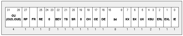
CP0 Status Register Usage
The layout of the CP0 status register is shown in Table 4 . This is taken from the IDT MIPS R4000 Microprocessor User's Manual. It includes a breakdown of the diagnostic field. We include it for your reference.
- The processor interrupt mask is changed via the following instruction sequence:
Since the above sequence is executed with interrupts enabled, it can be interrupted. As a consequence, interrupt handlers must restore c0_status to its original state before returning.
- The IE (Interrupt Enable) bit should not be used for disabling/enabling interrupts. Use the Intr5 .. 0 and Sw1 .. 0 bits instead.
- The Cu1 bit is used by the floating point support code, so it should not be changed.
Table 4 The MIPS II Status Register
Memory Management Support
Figure 13 is taken from the 1988 edition of Gary Kane's MIPS RISC Architecture. We include it for your reference.
For additional information about memory management in Apex, see "Memory Management" in the Ada Runtime Guide.
Figure 13 MIPS II/III/IV Virtual Memory Map
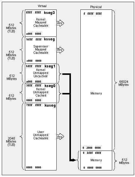
Apex Embedded currently does not support virtual (paged) memory. All code written for Apex Embedded runs in kernel mode in kseg0 (addresses 16#8000_0000# .. 16#9FFF_FFFF#) which is cached and directly mapped to physical memory locations 0 .. 16#1FFF_FFFF#. We do not support programs executing in user mode since they cannot access kseg0.
Accessing the Translation Lookaside Buffer (TLB)
The Apex microkernel does not support running applications in User or Supervisor mode, so it may appear that there is no reason to need or use the Translation Lookaside Buffer (TLB).
However, using kseg0 or kseg1 only allows access to the lowest 512 MB of physical address space of the 4 GB on the MIPS I processors or 64 GB on the MIPS II/III/IV/64 processors.
If you have memory or I/O devices beyond this 512 MB boundary (physical address 16#1FFF_FFFF#), you need to initialize the TLB and access them through one of the mapped segments such as kuseg.
Therefore, Rational Software Corporation supplies the package V_Tlb in the board_common view that gives you the ability to access the TLB from your program using pure Ada code.
The data structures and definitions for the TLB are declared in V_Cpu_Conf in the rational.ss subsystem.
Here is a brief summary of the TLB operations provided in V_Tlb:
The procedures Get and Put are intended to be used from within the debugger only, though there is nothing prohibiting you from using them in a program.
To be able to use V_Tlb.Get and V_Tlb.Put from within the debugger, simply With V_Tlb in one of your compilation units and they are included in your program when you link.
Example Specification of V_TLB
Example Debugging Session
An example debugging session using V_Tlb.Get and V_Tlb.Put is shown in this section.
  -- This is the syntax for calling a subprogram
  -- in the debugger.

> p v_tlb.get()

  -- Be patient, user procedure calls with serial TDM
  -- take about 20 seconds.
Procedure completed normally.

  -- Print TLB entry four

> p v_tlb.tlb(4)
pagemask: RECORD
    r1:   0
    mask: page_4k
    r2:   0
entryhi:  RECORD
    vpn2: 8
    r1:   0
    asid: 0
entrylo0: RECORD
    r1:  0
    pfn: 30000
    c:   cacheable_noncoherent
    d:   false
    v:   true
    g:   true
entrylo1: RECORD
    r1:  0
    pfn: 30001
    c:   cacheable_noncoherent
    d:   false
    v:   true
    g:   true

  -- Modify the first page frame address of the pair

> v_tlb.tlb(4).entrylo0.pfn := 16#20000#

  -- Modify the second page frame address of the pair

> v_tlb.tlb(4).entrylo1.pfn := 16#20001#
  -- Make sure it's now what we want.
  -- Print it out again.

> p v_tlb.tlb(4)
pagemask: RECORD
    r1:   0
    mask: page_4k
    r2:   0
entryhi:  RECORD
    vpn2: 8
    r1:   0
    asid: 0
entrylo0: RECORD
    r1:  0
    pfn: 20000
    c:   cacheable_noncoherent
    d:   false
    v:   true
    g:   true
entrylo1: RECORD
    r1:  0
    pfn: 20001
    c:   cacheable_noncoherent
    d:   false
    v:   true
    g:   true

  -- Write back all the TLB entries (including the one
  -- we modified)

> p v_tlb.put()
Procedure completed normally.
General Machine Code Precautions
Machine Code Routines with Implicit_Code(OFF)
pragma Implicit_Code(OFF) causes the compiler to not emit the preamble code such as instructions used to save the nonvolatile registers on the stack.
Normally, for every procedure, the compiler emits a data structure read by the runtime that specifies which registers were stored on the stack. If the Implicit_Code(OFF) pragma is used, the data structure emitted tells the runtime it has no knowledge of the stack contents for that frame, therefore the runtime cannot unwind that frame.
The result of this is that machine code routines using pragma Implicit_Code(OFF), do not propagate to the caller exceptions raised by machine code instructions or by any routines called by these routines.
Consider the following example:
with machine_code;
with v_cpu_conf;
procedure raise_if_greater(a,b: integer) is
    use machine_code;
    pragma implicit_code(off);
begin
    code_3'(sltu, t0, b'ref, a'ref); -- t0 <- a > b
    code_3'(beq, t0, zero, ok'ref);  -- branch if not (a > b)
    -- this should raise a NUMERIC_ERROR exception
    code_1'(break, +(v_cpu_conf.BREAK_OVERFLOW * 16#400#));
  << ok >>
    code_3'(addiu, sp, sp, -8); -- create a frame
    code_2'(sw, ra, base(sp));  -- save the return address
    -- another_routine may raise an exception
    code_1'(jal, another_routine'ref);
    code_2'(lw, ra, base(sp));    -- restore the return address
    code_3'(addiu, sp, sp, +8);   -- discard the frame
end;
If a > b or Another_Routine raises an exception, the RTS panics because it is not able to find enough information about the stack's contents to unwind it properly.
Note: Another_Routine may or may not be a machine code routine.
Accessing Memory Mapped I/O
Because of the MIPS architecture, several precautions must be observed when dealing with I/O ports.
Address Space
I/O ports must only be accessed through an uncached address space. Since Apex does not use kuseg or kseg2, this implies that all accesses must go through kseg0 which has the address range 16#A000_0000# .. 16#BFFF_FFFF#.
The Write Buffer
Most MIPS based boards contain a write-buffer. In some cases, the write buffer is on-chip. While it does improve performance dramatically, it can cause problems for memory-mapped I/O.
To insure data integrity, most write-buffer implementations insure that all pending memory-writes are completed before any memory-reads can. If this not the case for your board, you must flush the write-buffer before reading any I/O register whose contents depend on previous writes. Flushing the write-buffer is board implementation dependent, so you must find out how to do it.
To increase performance, some write-buffer implementations coalesce partial-word writes before writing to memory. For example, consider an algorithm that zeroes out memory by writing a zero to each byte, a byte at a time. A big performance gain is achieved if the write-buffer does a single word write to memory instead of four single byte writes to successive addresses. However, this can cause problems for memory-mapped I/O. For example, if the same memory-mapped register is written several times in a row, only the last write is actually be performed. If your board has this type of write-buffer and you have registers that require making several successive writes to a single address, you must flush the write-buffer between writes.
Improving Caching Performance - MIPS I Family
The following are covered in this section:
- MIPS I Caching Overview
- Cache Collisions
- Cache Collision Avoidance
- Collision Avoidance With the Apex Kernel
- Data Cache Collision Avoidance
MIPS I Caching Overview
The MIPS I architecture cache structure is direct mapped, as opposed to a multi-way-set-associative or a fully-associative cache. This means that every address in memory is mapped to exactly one location in the cache.
The relationship is very simple. For example, the Sanders STAR MVP board has 128K of data cache and 128K of instruction cache. Addresses 16#8000_0000# .. 16#8001_FFFF# are mapped to locations the 16#0_0000# .. 16#1_FFFF# of the cache. Addresses 16#8002_0000# .. 16#8003_FFFF# are again mapped to cache addresses 16#0_0000# .. 16#1_FFFF#, and so on.
Cache Collisions
Cache collisions occur whenever a cache miss occurs and decrease performance because the requested word must now be read from main memory.
Consider the following worst-case scenario:
Routine A, is in a loop calling routines B and C. Routine B is located at address 16#8004_0000# and routine C is located at address 16#8006_0000#.
with A;
with B;
procedure A is
begin
    while not_done loop
        B;
        C;
    end loop;
end A;
Whenever B is called, it gets cache misses for each of its instruction fetches because C's code is currently in the cache. Likewise, whenever C is called, it gets cache misses for its instruction fetches because B's instructions are in the cache.
Cache Collision Avoidance
Cache collisions can be avoided by insuring that highly used library units do not occupy the same position in cache. By either understanding your code very well, or using the profiling tool, you can determine most highly used units.
Once you have this information, change the linker options file so that these units either a) occupy their own section of cache shared with no other units, or b) occupy a section of cache shared with infrequently used units. Performance improvements of 15 percent or more for large programs are not unusual.
Rational Software Corporation recommends option a) because it is easier for you to manage. First, determine the total size of the text sections for the highly used units. Second, arrange a linker options file that places these units in their own section of cache.
For example, suppose that routines B and C are the most highly used units, and that they each have 16#1000# bytes in their text sections. Here is an excerpt from the linker options file:
...
ORIGIN 080040000
...
GROUP program_text1 IS
    A'text;
    B'text;
    text;
END GROUP;
FOR program_text1 USE AT 080041000 .. 080060FFF;
GROUP program_text2 IS
    text;
END GROUP;
FOR program_text2 USE AT 080063000 .. 080080FFF;
GROUP program_text3 IS
    text;
END GROUP;
FOR program_text3 USE AT 080083000 .. 0800A0FFF;
...
Notice the use of the text keyword in the three groups. This tells the linker to place as much of the remaining text sections in the space allowed as possible. It continues to place as many text sections in the groups until it either runs out of text to put in, or runs out of room in the last group containing a text keyword (in which case an error message is printed).
Also notice how a 16#2000# byte hole, namely cache addresses 16#0_1000# .. 16#0_2FFF#, has been created in the cache that only routines A and B can be placed in.
You can take this technique only so far. The larger the hole you create, the more the remaining units overlap in the cache, thus decreasing the performance of those units. You can determine the point of decreasing returns by gradually increasing the size of the hole, including more of the frequently used units and monitoring the performance.
Collision Avoidance With the Apex Kernel
If your program makes extensive use of the kernel services, it may be that by profiling the kernel together with your program, you can come up with a linker options file for the kernel that improves performance further. The techniques used are identical to the above, with the exception that the profiling configuration file must be changed to include the kernel's address space.
If units in the kernel are more highly used than routines in your program, you may want to place them in sections of the cache that are neither used by your program nor by other units in the kernel.
Data Cache Collision Avoidance
This same technique can also be used for the data cache, though it's more difficult to find out what data is accessed most often.
In this case, you have multiple groups of Program_Const, Program_Data_Image, and Program_Data_Bss, whichever one(s) you are trying to protect in the cache.
Improving Caching Performance - MIPS II/III/IV/64 Family
The following are covered in this section:
- MIPS II/III/IV/64 Caching Overview
- Cache Collisions
- Cache Collision Avoidance
- Collision Avoidance With the Apex Kernel
- Data Cache Collision Avoidance
MIPS II/III/IV/64 Caching Overview
In some implementations of the MIPS II/III/IV/64 architecture, the cache structure is direct mapped, as opposed to a multi-way-set-associative or a fully-associative cache. This means that every address in memory is mapped to exactly one location in each level of cache (primary and secondary).
For a direct mapped cache, the relationship is very simple. For example, assume that your R4400 board has 128K of secondary data cache and 128K of secondary instruction cache. Addresses 16#8000_0000# .. 16#8001_FFFF# are mapped to locations the 16#0_0000# .. 16#1_FFFF# of the cache. Addresses 16#8002_0000# .. 16#8003_FFFF# are again mapped to cache addresses 16#0_0000# .. 16#1_FFFF#, and so on.
In other implementations of the MIPS II/III/IV/64 architecture (for example, the R4600), the primary cache is two-way set associative. Because of this, cache collisions are less likely, but still occur. The larger size of the primary cache in newer chip implementations make them candidates for collision avoidance.
Cache Collisions
Cache collisions occur whenever a cache miss occurs and decrease performance because the requested word must now be read from main memory.
Consider the following worst-case scenario:
Routine A, is in a loop calling routines B and C. Routine B is located at address 16#8004_0000# and routine C is located at address 16#8006_0000#.
with A;
with B;
procedure A is
begin
    while not_done loop
        B;
        C;
    end loop;
end A;
Whenever B is called, it gets cache misses for each of its instruction fetches because C's code is currently in the cache. Likewise, whenever C is called, it gets cache misses for its instruction fetches because B's instructions are in the cache.
Note that for a two-way set associative cache, there must be three heavily used routines occupying the same location in cache for there to be a collision problem.
Cache Collision Avoidance
Because some MIPS II/III/IV/64 chips have a small primary cache, this technique centers around cache collision avoidance in the secondary cache, which is always directly mapped.
Cache collisions can be avoided by insuring that highly used library units do not occupy the same position in cache. By either understanding your code very well, or using the profiling tool, you can determine most highly used units.
Once you have this information, change the linker options file so that these units either a) occupy their own section of cache shared with no other units, or b) occupy a section of cache shared with infrequently used units. Performance improvements of 15 percent or more for large programs are not unusual.
Rational Software Corporation recommends option a) because it is easier for you to manage. First, determine the total size of the text sections for the highly used units. Second, arrange a linker options file that places these units in their own section of cache.
For example, suppose that routines B and C are the most highly used units, and that they each have 16#1000# bytes in their text sections. Here is an excerpt from the linker options file:
...
ORIGIN 080040000
...
GROUP program_text1 IS
    A'text;
    B'text;
    text;
END GROUP;
FOR program_text1 USE AT 080041000 .. 080060FFF;

GROUP program_text2 IS
    text;
END GROUP;
FOR program_text2 USE AT 080063000 .. 080080FFF;

GROUP program_text3 IS
    text;
END GROUP;
FOR program_text3 USE AT 080083000 .. 0800A0FFF;
...
Notice the use of the text keyword in the three groups. This tells the linker to place as much of the remaining text sections in the space allowed as possible. It continues to place as many text sections in the groups until it either runs out of text to put in, or runs out of room in the last group containing a text keyword (in which case an error message is printed).
Also notice how a 16#2000# byte hole, namely cache addresses 16#0_1000# .. 16#0_2FFF#, has been created in the cache that only routines A and B can be placed in.
You can take this technique only so far. The larger the hole you create, the more the remaining units overlap in the cache, thus decreasing the performance of those units. You can determine the point of decreasing returns by gradually increasing the size of the hole, including more of the frequently used units and monitoring the performance.
Collision Avoidance With the Apex Kernel
If your program makes extensive use of the kernel services, it may be that by profiling the kernel together with your program, you can come up with a linker options file for the kernel that improves performance further. The techniques used are identical to the above, with the exception that the profiling configuration file must be changed to include the kernel's address space.
If units in the kernel are more highly used than routines in your program, you may want to place them in sections of the cache that are neither used by your program nor by other units in the kernel.
Data Cache Collision Avoidance
This same technique can also be used for the data cache, though it's more difficult to find out what data is accessed most often.
In this case, you have multiple groups of Program_Const, Program_Data_Image, and Program_Data_Bss, whichever one(s) you are trying to protect in the cache.
Honeywell RH32 CPU Usage ModelThe following sections describe how the RH32 and its floating point units are set up and used by TDM and the kernel. It also lists precautions to be taken when writing machine code.
Note: In the discussions that follow, the user should also refer to the "Radiation Hardened 32 Bit Processor (RH32) Software Programmer's Manual,YG9562ASPM, Revision B." published by the Honeywell Space and Strategic Systems Organization.
Overview
The RH32 is a 32-bit RISC processor, with 32 general purpose registers, and a floating point unit with 16 floating point registers capable of holding either a 32-bit or 62-bit IEEE floating point value. The RH32 uses big-endian byte order only.
The RH32 architecture supports two modes of execution - user and kernel. Programs running in user mode are restricted as to what memory and coprocessors can be accessed. The Apex kernel however, runs all programs in kernel mode only, which provides direct access to the underlying hardware.
Initialization
Because the RH32 architecture is fixed in many ways, and since Apex Embedded does not use virtual memory, very little initialization needs to be performed to get the processor going. Initialization consists mainly of initializing the CPU status register and initializing the caches.
Floating Point Coprocessor (FPC) Support
The RH32's FPC supports the basic arithmetic operations on floats: +, -, *, /, abs, unary - and some format conversions. The FPP is capable of handling only operations on numbers in a restricted size range, a smaller range than the IEEE specification. In circumstances where intermediate values exceed the range supported by the FPP, a trap is taken, and typically a Constraint_Error is raised in the application at the point where the floating point error is detected.
CPU Status Register Usage
The layout of the CPU status register is shown in Figure 14. This figure is taken from the 1988 edition of Gary Kane's MIPS RISC Architecture. It includes a breakdown of the diagnostic field. We include it for your reference.
Figure 14 The MIPS Status Register
- The processor interrupt mask is changed via the following instruction sequence:
Since the above sequence is executed with interrupts enabled, it can be interrupted. As a consequence, interrupt handlers must restore Cpu_Status to its original state before returning.
The Current Interrupt Enable bit should not be used for disabling/enabling interrupts. Use the Intr7 .. 0 bits instead. The Old Interrupt Enable bit is lost when an interrupt occurs, so it cannot be relied upon to stay the same between any two instructions unless all interrupts are disabled. Memory Management Support
Apex Embedded does not support virtual (paged) memory. All code written for Apex Embedded runs in kernel mode and must refer to addresses in kseg0 or kseg1. Apex Embedded does not support programs executing in user mode since they cannot access kseg0.
For additional information about memory management in Apex, see "Memory Management" in the Ada Runtime Guide.
General Machine Code Precautions
Machine Code Routines with Implicit_Code(OFF)
pragma Implicit_Code(OFF) causes the compiler to not emit the preamble code such as instructions used to save the nonvolatile registers on the stack.
Normally, for every procedure, the compiler emits a data structure read by the runtime that specifies which registers were stored on the stack. If the Implicit_Code(OFF) pragma is used, the data structure emitted tells the runtime it has no knowledge of the stack contents for that frame, therefore the runtime cannot unwind that frame.
The result of this is that machine code routines using pragma Implicit_Code(OFF), do not propagate to the caller exceptions raised by machine code instructions or by any routines called by these routines.
Consider the following example:
with machine_code;
with v_cpu_conf;
procedure raise_if_greater(a,b: integer) is
    use machine_code;
    pragma implicit_code(off);
begin
    code_3'(bgt, b'ref, a'ref, ok'ref);-- branch if not (a > b)
    -- this should raise a NUMERIC_ERROR exception
    code_1'(trap, +(v_cpu_conf.BREAK_OVERFLOW * 16#400#));
  << ok >>
    code_3'(addiu, sp, sp, -8); -- create a frame
    code_2'(st, ra, base(sp));  -- save the return address
    -- another_routine may raise an exception
    code_1'(call, another_routine'ref);
    code_2'(ld, ra, base(sp));    -- restore the return address
    code_3'(addiu, sp, sp, +8);   -- discard the frame
end;
If a > b or Another_Routine raises an exception, the RTS panics because it is not able to find enough information about the stack's contents to unwind it properly. Note that Another_Routine may or may not be a machine code routine.
Mapped I/O
Because of the RH32 architecture, several precautions must be observed when dealing with I/O ports.
Address Space, Accessing I/O Ports
I/O ports must only be accessed through an uncached address space. This uncached space is generally designated by an address with the high order bit (31) being set. However, to ensure that accesses to hardware I/O ports bypass the cache you should use the getio and putio Machine_Code instructions. Getio and putio expand into several RH32 machine instructions; they accomplish the task of accessing I/O ports directly, bypassing the cache.
M68000 CPU Usage ModelRegister Conventions
Apex Ada observes the following conventions:
When interfacing to the C compiler observe the following conventions:
Parameter Passing
Apex Ada passes the first two scalar parameters in D2 and D3, and the first four floating-point parameters in FP0-FP3. The remaining parameters are passed on the stack with the last parameter at the highest address. (i.e. pushed in reverse order).
Each scalar parameter occupies a longword (4-byte) slot on the stack. If a parameter is smaller than a longword it is right-justified in its slot (i.e. the least significant bit is in the same location as it would be if a full longword were stored).
Each single-precision float parameter occupies a longword slot on the stack.
Each double-precision float parameter occupies a 8-byte slot. Padding may be inserted so that the offset from the SP is a multiple of 8.
If parameters are passed on the stack, then some stack space may also be reserved for parameters passed in registers as if they were passed on the stack (including any padding), but the total amount of space reserved will be reduced by 8-bytes. Thus a parameter that is passed on the stack is passed at an offset from the SP (before the call) which is the same as it would be if all the parameters were passed on the stack, less 8 bytes.
Apex Ada always passes structured parameters (arrays, records) by reference.
Interrupt Stack Switching and Processor States
The high-end M68000 family processors (MC68020/30/40/60) have three hardware stack registers, USP, MSP and ISP. The low end M68000 family processors (MC68000/10 and CPU32) have only two hardware stack registers, USP and SSP. For this discussion, SSP is equivalent to ISP. When an instruction uses the stack, it uses the A7 register. However, the A7 register does not really exist. The processor maps each use of the A7 register onto one of the hardware stack registers depending on the current mode of the processor, as determined by the S and M bits of the Status Register (SR). The low-end processor have no M bit in the Status Register. Therefore, discussion of any processor mode where M=1 is inapplicable to these processor since, in effect, the M bit is always zero.
Table 5 Stack Register Assigned to Each Privilege
SM Stack Register
00 USP
10 ISP
01 USP
11 MSP (MC68020/30/40 Only
The processor changes modes in response to an interrupt or internal exception (a TRAP instruction) occurs. Table 6 shows these transitions:
Table 6 Interrupt/Exception Transitions
Interrupt Internal Exception
SM stack => SM stack SM stack => SM stack
00 USP 10 ISP 00 USP 10 ISP
10 ISP 10 ISP 10 ISP 10 ISP
01 USP 10 ISP 01 USP 11 MSP
11 MSP 10 ISP 11 MSP 11 MSP
The kernel and VADSexec tasks make use of four stacks:
Kernel Stack
When the kernel is executing, it uses its own stack. The kernel stack size is controlled by the Krn_Stack_Size configuration parameter. For additional information on Krn_Stack_Size, see "M68000 Family Kernel Configuration Components" in the Configuration Guide for VADSexec.
Interrupt Stack
This is a system-wide stack that may be shared by all ISRs. There is a considerable space savings that can be obtained if all ISRs use one stack. The interrupt stack size is controlled by the Intr_Stack_Size kernel configuration parameter. For additional information on Intr_Stack_Size, see "M68000 Family Kernel Configuration Components" in the Configuring Rational Exec Guide.
Task User Stack
Each task has its own private user stack, unless Supervisor_Tasks_Enabled is True, in which case the tasks do not need a user stack, since they only use the task supervisor stack. The default task stack size is set by the Task_Stack_Size_Default parameter of pragma Main. For more information about Task_Stack_Size_Default, see that section of the discussion of "Pragma Main" in the Ada Compiler Reference.
Task Supervisor Stack
Each task has its own private supervisor stack. Kernel services also use the current tasks supervisor stack. Kernel services normally do not need more than 500 bytes. However, additional stack is needed when nested tasks are terminated.
The kernel takes care of the kernel stack, so this discussion is going to focus on the execution of application code and the other three stacks: the interrupt stack, the task user stack and the task supervisor stack. The term application code refers to all execution that is not part of the kernel.
A task can have one of four stack configurations,depending on the setting of the S and M bits in the SR register while the task is executing. A configuration describes which stack is pointed to by each M68000 stack register during execution of application code. The four configurations are shown in Table 7.
Each line of Table 7 shows one stack configuration. The S and M bit settings during task execution are determined by the kernel configuration variables Supervisor_Tasks_Enabled and Master_State_Enabled respectively.
Table 7 Stack Registers to VADSexec Stacks Mapping
SM USP ISP MSP
00 User Stack Supervisor Stack n/u
10 n/u Supervisor Stack n/u
01 User Stack Interrupt Stack Supervisor Stack
(MC68020/30/40 only)
11 n/u Interrupt Stack Supervisor Stack
(MC68020/30/40 only)
n/u = not used
Interrupt Stack [shared, system-wide]
User Stack [private, one per task]
Supervisor Stack [private, one per task]
The following four sections describe each of these configurations, giving the advantages and disadvantages of each.
- SM = 00: User Tasks, Master State Not Enabled
- SM = 10: Supervisor Tasks, Master State Not Enabled
- SM = 01: User Tasks, Master State Enabled (MC68020/30/40/60 Only)
- SM = 11: Supervisor Tasks, Master State Enabled (MC68020/30/40/60 Only)
SM = 00: User Tasks, Master State Not Enabled
In this state, an interrupt or internal exception switch to state SM = 10 and begin using the ISP as the stack (A7). For each task the ISP points at the task's private supervisor stack when the ISR begins executing. This means that each task's supervisor stack must contain enough space to handle stack usage by the worst case nesting of interrupts. If a system has many tasks, this memory requirement can become substantial. If a system has only a few tasks, then the supervisor stack overhead per task may not be big enough to worry about.
A common method to reduce the memory requirement of these supervisor stacks is to have all the ISRs share a common interrupt stack. There are two ways to do this, each involves switching stacks after the interrupt. One is to run with master state enabled, SM = 01. This is the most efficient and fastest way to share a system-wide interrupt stack, because the switch happens in hardware. This is discussed in the next section. The second method is to call Isr_Enter to switch stacks.
There are some performance gains to being able to handle interrupts on a task's private supervisor stack. Switching to a system-wide interrupt stack introduces overhead, whether the hardware does it or Isr_Enter does it. For example, the MC68020 timings indicate that it requires 15 more clocks to handle an interrupt if master state is enabled.
An ISR can call Isr_Enter to switch from the task's supervisor stack to the system-wide interrupt stack. However, before the switch takes place, a certain amount of supervisor stack space is used and there must be room on each task's supervisor stack for this space.
The required size for a task supervisor stack is calculated by adding together three components: (1) the worst case supervisor stack usage just prior to the first interrupt, (2) the worst case supervisor stack usage to handle the first interrupt and (3) the worst case supervisor stack usage for nested interrupts.
Since an interrupt can occur in the kernel, which executes on the current task's supervisor stack, the worst case supervisor stack usage just prior to the first interrupt is the kernel's maximum stack use, which is approximately 500 bytes.
When the first interrupt occurs, we can use this much stack space:
This is worst case stack usage for the initial interrupt of a task. Just prior to switching to the interrupt stack, another higher priority interrupt could arrive. If that occurred, it does not need 40 bytes, because we know that Isr_Enter is not doing a coprocessor operation. Therefore, the MC68020 would push a four word stack frame onto the stack, which would use 8 bytes instead of 20. This reduces the worst case stack requirements for any nested interrupts from 40 to 28 bytes per nested interrupt.
If the embedded system hardware can generate interrupts at levels 1, 3 and 6, then our final calculation would be:
SM = 10: Supervisor Tasks, Master State Not Enabled
In this state, each task executes exclusively in supervisor state and has only one stack (the supervisor stack). The ISP that points to the supervisor stack is always the active stack register.
An interrupt or internal exception pushes an exception frame onto the stack and starts executing at the interrupt or exception handler. This state is much like state SM = 00, in that every task's supervisor stack must contain enough extra space to handle the worst case of interrupt nesting.
Like state SM = 00, if you want all the ISRs to share a common interrupt stack, you must switch stacks with software, calling Isr_Enter at the beginning of each ISR. It is more efficient to enable master state and have the hardware switch stacks automatically (see SM = 11: Supervisor Tasks, Master State Enabled).
As mentioned in the discussion on state SM = 00, it is faster not to switch stacks when an interrupt occurs but to have each ISR use the supervisor stack of the task that is interrupted. If a system has only a few tasks, the supervisor stack space overhead per task may not be big enough to be a concern.
SM = 01: User Tasks, Master State Enabled (MC68020/30/40/60 Only)
In this state there are three stacks, the task's user stack where all stack usage by application code takes place, the task's supervisor stack for kernel services and the interrupt stack shared by all ISRs.
An interrupt causes the processor to push an exception frame on the task's supervisor stack (pointed to by MSP) and then switch to the ISP and push a throwaway exception frame onto that stack. An internal exception (TRAP instruction, zero divide) pushes an exception frame onto the task's supervisor stack and continues to execute using that stack.
As mentioned in the previous section, if you are going to have one common interrupt stack shared by all ISRs, having master state enabled is the most efficient way to do it. You still must have a supervisor stack for each task but it must only be big enough to handle the needs of kernel services (500 bytes) and one instance of the worst case interrupt stack frame (20 bytes for a Coprocessor Mid-instruction exception stack frame), Total bytes needed: 520.
SM = 11: Supervisor Tasks, Master State Enabled (MC68020/30/40/60 Only)
In this state there are two stacks, the task's supervisor stack, used by both application code and internal exception handling and the interrupt stack, shared by all ISRs.
An interrupt first pushes an exception frame on the task's supervisor stack (pointed to by MSP) and then switches to the interrupt stack (pointed to by ISP) and pushes a throwaway exception frame onto that stack. An internal exception (a TRAP instruction, zero divide) pushes an exception frame on the task's supervisor stack and continues to execute using that stack. This state is similar to state SM = 01.
For additional information, see ISRs and M68000 Family Interrupt Levels and Installing an ISR in the Exception Vector Table.
i386 Family CPU Usage ModelThis section describes how the kernel sets up and uses the i386 Family CPU registers and data structures.
During initialization, the Runtime System places the i386 into protected mode. The model of memory organization is a `flat' address space consisting of a single array of up to 4 gigabytes. A pointer into this flat address space is a 32-bit unsigned integer in the range 0 to 4,294,967,295.
By default, the kernel configuration parameter Page_Protection_Enabled is set to True, whereby the runtime system enables paging, so that linear addresses map directly to their physical addresses. A user-configurable memory-map table indicates which pages are present. Attempting to access a non-existent page causes a page fault.
Kernel services and Interrupt Service Routines (ISRs) execute at privilege level 0 (greatest privilege). The user program executes at privilege level 3 (lowest). Control is transferred from the user program to kernel services via an interrupt gate. Call gates are not used. However, (in the current implementation) the kernel address space is not protected; it can be accessed from the user program without privilege violation.
The I/O privilege level is 3 (IOPL in EFLAGS). Therefore, the user program can execute any I/O related instruction: CLI, STI, IN, INS, OUT or OUTS without privilege violation.
The i386 Family tasking facility is not used for Ada tasking. The kernel and user programs execute within a single i386 task. However, kernel service, exception and external interrupts automatically switch to the level 0 stack segment and stack pointer specified in the i386 task state segment (TSS). The TSS is set up during kernel initialization.
For floating point operations, the presence of a floating point coprocessor is assumed. No floating point emulation software is provided. However, if no floating point operations are performed, a coprocessor is not required.
Details on the setup of the CPU registers and data structures follow.
Segment Registers
CS kernel code (RPL = 0) or user code (RPL = 3) selector
SS kernel data (RPL = 0) or user data (RPL = 3) selector
DS, ES user data (RPL = 3) selector
FS, GS not used
EFLAGS
CR0
CR1
Not used.
CR2, CR3
DR0 - DR7
Debug registers used by TDM.
TR6, TR7
Test registers are not used.
GDT Entries
0 NULL
1 .. 19 NULL or monitor entries
20 kernel code, DPL = 0
21 kernel data and stack, DPL = 0
22 user code, DPL = 3
23 user data and stack, DPL = 3
24 TSS
Code, data and stack segments address entire linear address space
The base and length of the monitor entries copied into the GDT are defined by the configuration parameters Monitor_Gdt_Base and Monitor_Gdt_Length.0 .. 2 ** 32 - 1
LDT
Null, not used.
TSS
The kernel and user program share the same TSS. The TSS is initialized at startup and never changed thereafter.
TSS fields:
ss0 kernel data selector
esp0 top of kernel/ISR stack
All other fields are set to NULL/0.
IDT
The base and length of the interrupt descriptor table are defined by the Idt_Base and Interrupt_Vector_Size configuration parameters. Since the table is updated during run-time execution it must be located in RAM.
All IDT descriptors are i386 interrupt gates are formatted as follows:
selector = kernel code selector
offset = 32 bit linear address of interrupt handler
type = i386 interrupt gate (interrupt handler is entered with interrupts disabled)
Interrupt handlers execute in the kernel code segment. When the user program is interrupted, SS:ESP is set to ss0:esp0 found in TSS.
| Rational Software Corporation http://www.rational.com support@rational.com techpubs@rational.com Copyright © 1993-2002, Rational Software Corporation. All rights reserved. |